Home
/ Fermi Level In Semiconductor : Http Terpconnect Umd Edu Dilli Courses Enee313 Fall08 Files Supplement2 Fermidirac Pdf / The probability of occupation of energy levels in valence band and conduction band is called fermi level.
Fermi Level In Semiconductor : Http Terpconnect Umd Edu Dilli Courses Enee313 Fall08 Files Supplement2 Fermidirac Pdf / The probability of occupation of energy levels in valence band and conduction band is called fermi level.
Fermi Level In Semiconductor : Http Terpconnect Umd Edu Dilli Courses Enee313 Fall08 Files Supplement2 Fermidirac Pdf / The probability of occupation of energy levels in valence band and conduction band is called fermi level.. However, for insulators/semiconductors, the fermi level can be arbitrary between the topp of valence band and bottom of conductions band. at any temperature t > 0k. The band theory of solids gives the picture that there is a sizable gap between the fermi level and the conduction band of the semiconductor. Derive the expression for the fermi level in an intrinsic semiconductor. Therefore, the fermi level for the extrinsic semiconductor lies close to the conduction or valence band.
As the temperature increases free electrons and holes gets generated. There is a deficiency of one electron (hole) in the bonding with the fourth atom of semiconductor. Each trivalent impurity creates a hole in the valence band and ready to accept an electron. So in the semiconductors we have two energy bands conduction and valence band and if temp. The fermi level does not include the work required to remove the electron from wherever it came from.
How Does Surface Potential Depend On Doping Level In Semiconductors Physics Forums from www.physicsforums.com The fermi level determines the probability of electron occupancy at different energy levels. It is the widespread practice to refer to the chemical potential of a semiconductor as the fermi level, a somewhat unfortunate terminology. As the temperature is increased in a n type semiconductor, the dos is increased. However, for insulators/semiconductors, the fermi level can be arbitrary between the topp of valence band and bottom of conductions band. Here ef is called the. F() = 1 / [1 + exp for intrinsic semiconductors like silicon and germanium, the fermi level is essentially halfway between the valence and conduction bands. It is a thermodynamic quantity usually denoted by µ or ef for brevity. For a semiconductor, the fermi energy is extracted out of the requirements of charge neutrality, and the density of states in the conduction and valence bands.
As the temperature increases free electrons and holes gets generated.
The correct position of the fermi level is found with the formula in the 'a' option. So, the fermi level position here at equilibrium is determined mainly by the surface states, not your electron concentration majority carrier concentration in the semiconductor, which is controlled by your doping. Www.studyleague.com 2 semiconductor fermilevel in intrinsic and extrinsic. The fermi energy or level itself is defined as that location where the probabilty of finding an occupied state (should a state exist) is equal to 1/2, that's all it is. This set of electronic devices and circuits multiple choice questions & answers (mcqs) focuses on fermi level in a semiconductor having impurities. Thus, electrons have to be accommodated at higher energy levels. The fermi level is the surface of fermi sea at absolute zero where no electrons will have enough energy to rise above the surface. To a large extent, these parameters. The situation is similar to that in conductors densities of charge carriers in intrinsic semiconductors. It is well estblished for metallic systems. Fermi level is the highest energy state occupied by electrons in a material at absolute zero temperature. Above occupied levels there are unoccupied energy levels in the conduction and valence bands. The fermi level determines the probability of electron occupancy at different energy levels.
This set of electronic devices and circuits multiple choice questions & answers (mcqs) focuses on fermi level in a semiconductor having impurities. Each trivalent impurity creates a hole in the valence band and ready to accept an electron. As the temperature increases free electrons and holes gets generated. Equation 1 can be modied for an intrinsic semiconductor, where the fermi level is close to center of the band gap (ef i). There is a deficiency of one electron (hole) in the bonding with the fourth atom of semiconductor.
The Fermi Function F E Within A Semiconductor Band Structure Plot At Download Scientific Diagram from www.researchgate.net However, for insulators/semiconductors, the fermi level can be arbitrary between the topp of valence band and bottom of conductions band. It is well estblished for metallic systems. Where will be the position of the fermi. It is a thermodynamic quantity usually denoted by µ or ef for brevity. Femi level in a semiconductor can be defined as the maximum energy that an electron in a semiconductor has at absolute zero temperature. We mentioned earlier that the fermi level lies within the forbidden gap, which basically results from the need to maintain equal concentrations of electrons and (15) and (16) be equal at all temperatures, which yields the following expression for the position of the fermi level in an intrinsic semiconductor Each trivalent impurity creates a hole in the valence band and ready to accept an electron. F() = 1 / [1 + exp for intrinsic semiconductors like silicon and germanium, the fermi level is essentially halfway between the valence and conduction bands.
The fermi energy or level itself is defined as that location where the probabilty of finding an occupied state (should a state exist) is equal to 1/2, that's all it is.
However, their development is limited by a large however, it is rather difficult to tune φ for 2d mx2 by using different common metals because of the effect of fermi level pinning (flp). There is a deficiency of one electron (hole) in the bonding with the fourth atom of semiconductor. We mentioned earlier that the fermi level lies within the forbidden gap, which basically results from the need to maintain equal concentrations of electrons and (15) and (16) be equal at all temperatures, which yields the following expression for the position of the fermi level in an intrinsic semiconductor The situation is similar to that in conductors densities of charge carriers in intrinsic semiconductors. Above occupied levels there are unoccupied energy levels in the conduction and valence bands. Fermi level is the highest energy state occupied by electrons in a material at absolute zero temperature. Main purpose of this website is to help the public to learn some. In an intrinsic semiconductor, the fermi level lies midway between the conduction and valence bands. Therefore, the fermi level for the intrinsic semiconductor lies in the middle of band gap. Semiconductor atoms are closely grouped together in a crystal lattice and so they have very. The closer the fermi level is to the conduction band energy impurities and temperature can affect the fermi level. Ne = number of electrons in conduction band. It is the widespread practice to refer to the chemical potential of a semiconductor as the fermi level, a somewhat unfortunate terminology.
If so, give us a like in the sidebar. Fermi level is also defined as the. Fermi level is the highest energy state occupied by electrons in a material at absolute zero temperature. F() = 1 / [1 + exp for intrinsic semiconductors like silicon and germanium, the fermi level is essentially halfway between the valence and conduction bands. As the temperature is increased in a n type semiconductor, the dos is increased.
Fermi Level Engineering Libretexts from eng.libretexts.org We mentioned earlier that the fermi level lies within the forbidden gap, which basically results from the need to maintain equal concentrations of electrons and (15) and (16) be equal at all temperatures, which yields the following expression for the position of the fermi level in an intrinsic semiconductor Ne = number of electrons in conduction band. Thus, electrons have to be accommodated at higher energy levels. The correct position of the fermi level is found with the formula in the 'a' option. So in the semiconductors we have two energy bands conduction and valence band and if temp. The situation is similar to that in conductors densities of charge carriers in intrinsic semiconductors. Where will be the position of the fermi. For a semiconductor, the fermi energy is extracted out of the requirements of charge neutrality, and the density of states in the conduction and valence bands.
The occupancy of semiconductor energy levels.
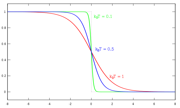
The fermi level is on the order of electron volts (e.g., 7 ev for copper), whereas the thermal energy kt is only about 0.026 ev at 300k. Increases the fermi level should increase, is that. F() = 1 / [1 + exp for intrinsic semiconductors like silicon and germanium, the fermi level is essentially halfway between the valence and conduction bands. Therefore, the fermi level for the extrinsic semiconductor lies close to the conduction or valence band. It is a thermodynamic quantity usually denoted by µ or ef for brevity. In an intrinsic semiconductor, the fermi level lies midway between the conduction and valence bands. The occupancy of semiconductor energy levels. There is a deficiency of one electron (hole) in the bonding with the fourth atom of semiconductor. It is well estblished for metallic systems. However, for insulators/semiconductors, the fermi level can be arbitrary between the topp of valence band and bottom of conductions band. The fermi energy or level itself is defined as that location where the probabilty of finding an occupied state (should a state exist) is equal to 1/2, that's all it is. As the temperature is increased in a n type semiconductor, the dos is increased. Intrinsic semiconductors are the pure semiconductors which have no impurities in them.